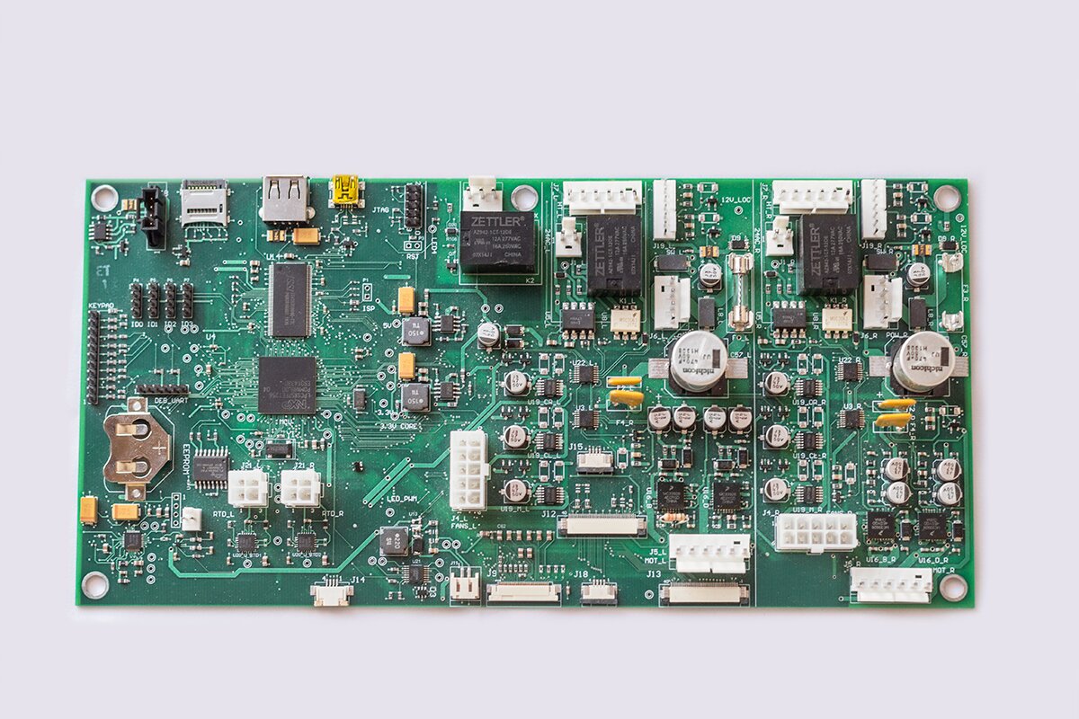
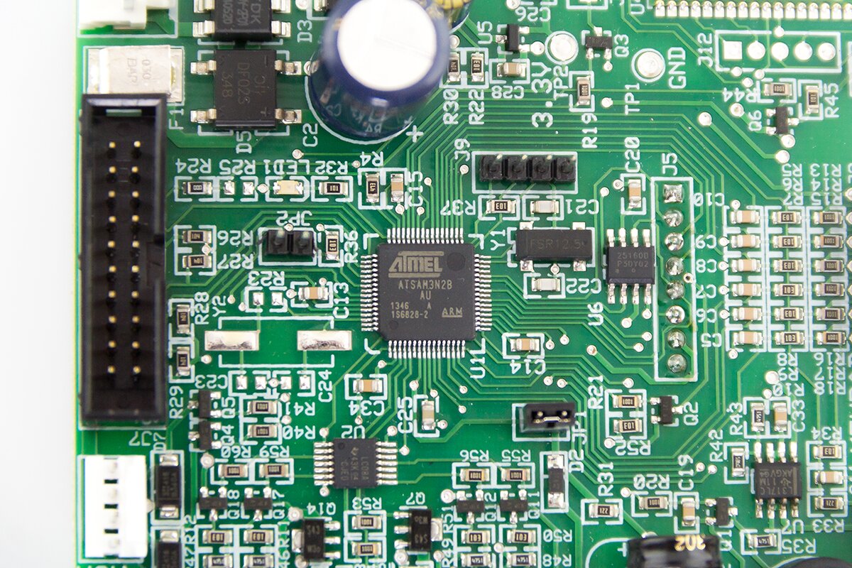
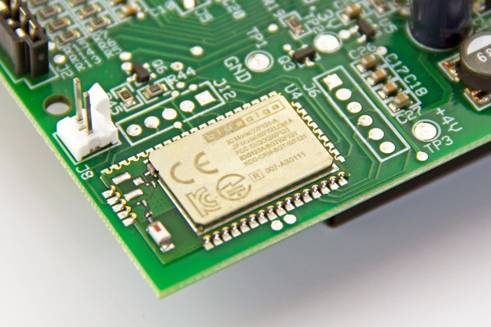
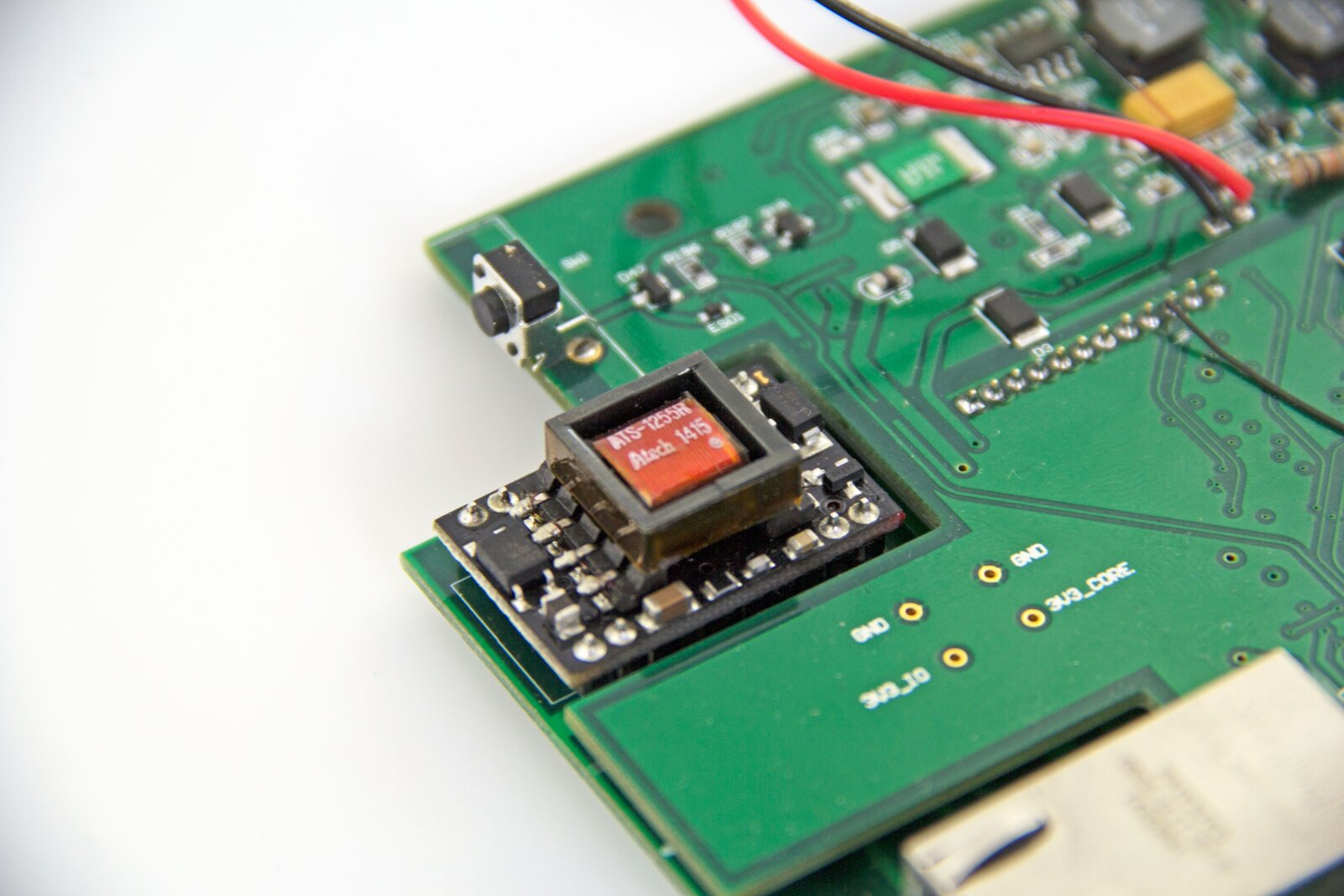
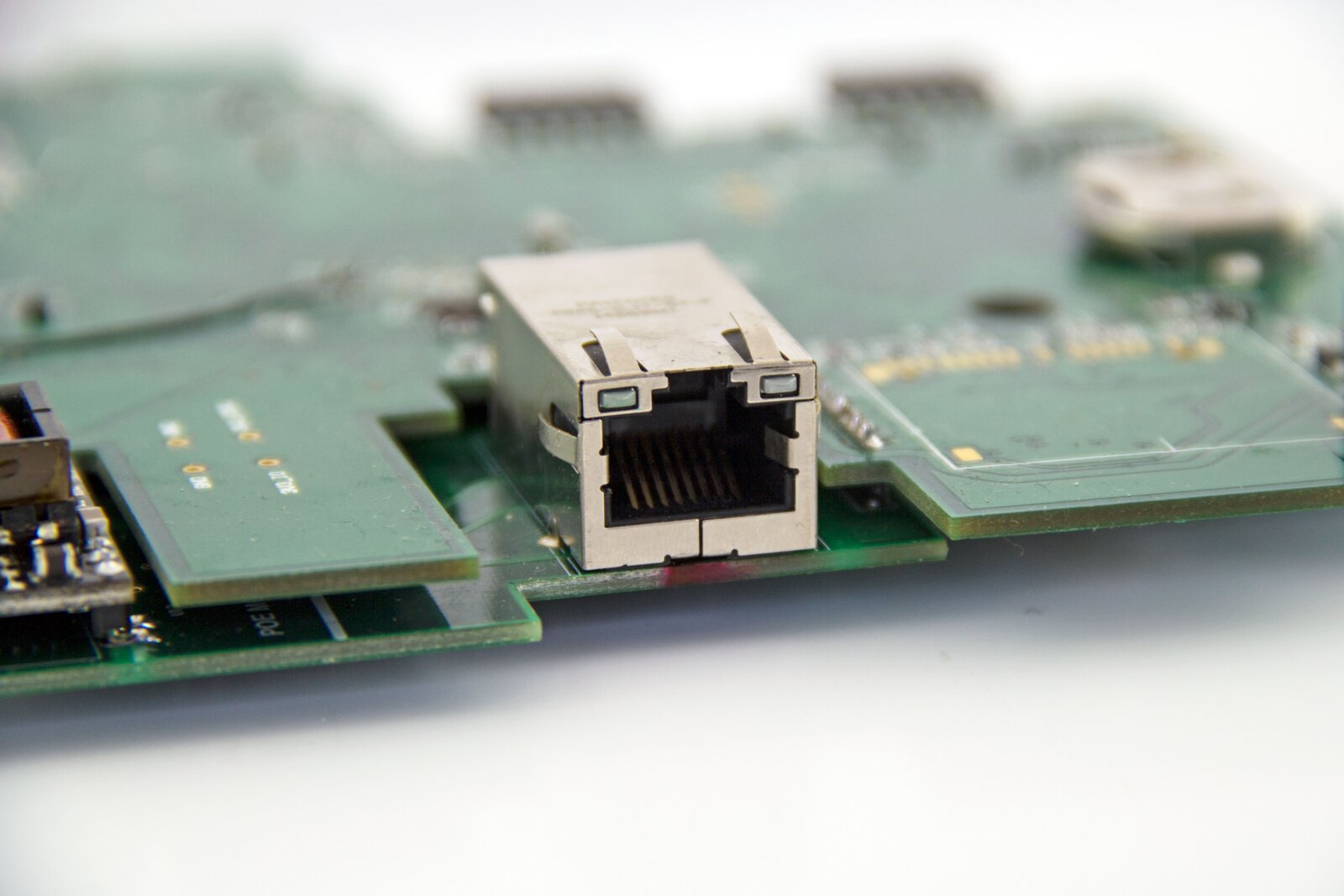
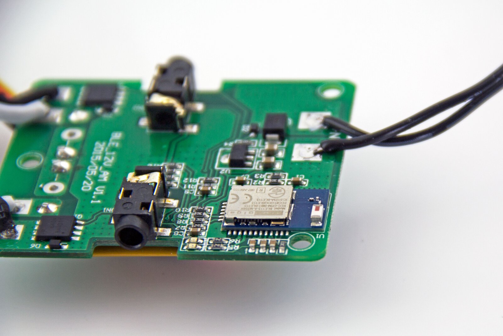
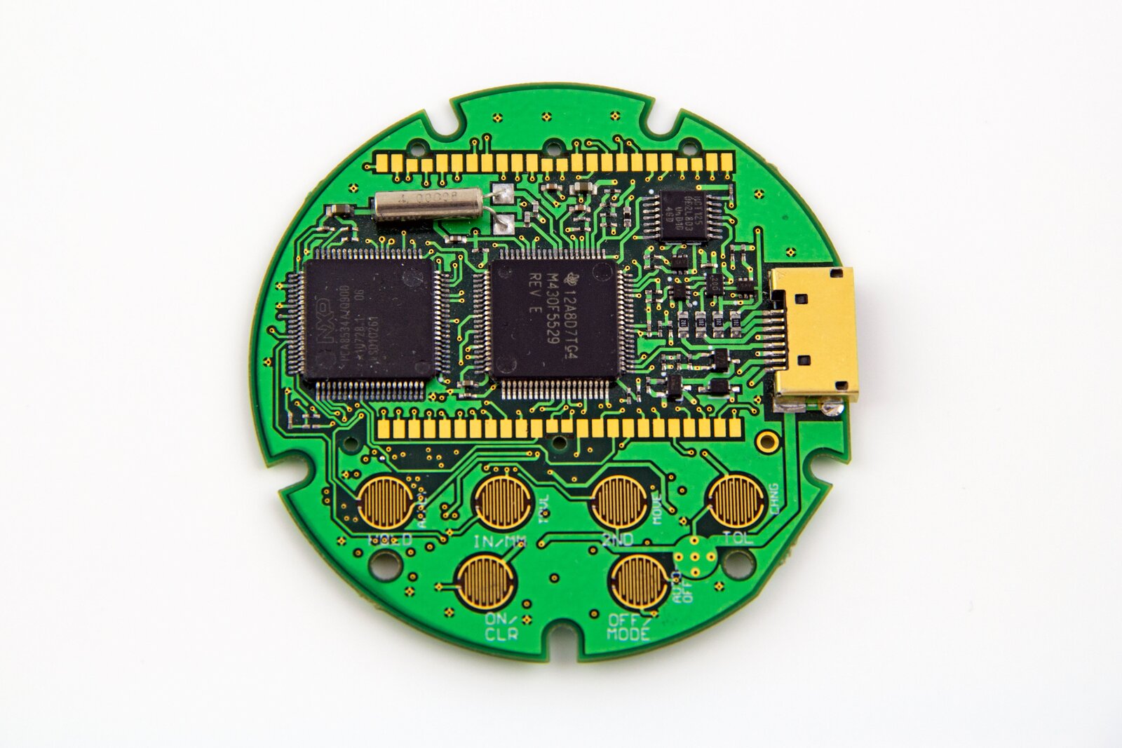
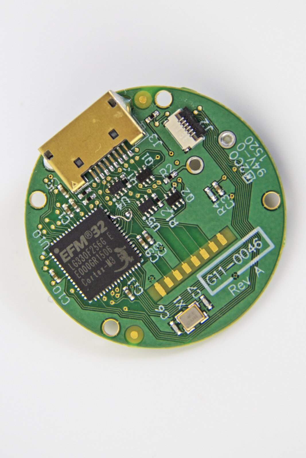
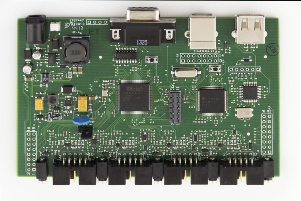
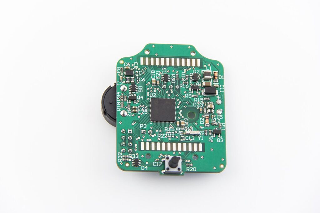
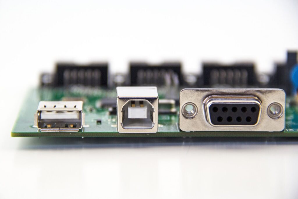
DMC can help you with your embedded hardware development from concept to market. We can also help redesign or debug issues with your existing system. Our areas of expertise in embedded hardware development include, but are not limited to:
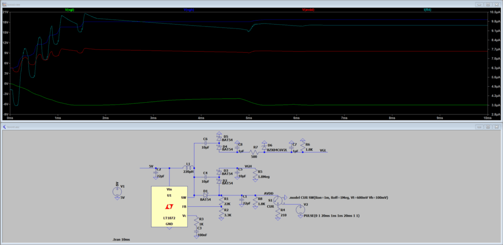
- Circuit calculation and simulation
- Digital and Analog Circuit Board Design
- Part selection for specific project needs, including cost-optimized design
- Multi-layered boards
- Prototyping
- Power electronics
- RF/EMI noise immunity
- ESD protection
- Low power consumption systems
- Wireless applications
- Mobile systems
- Functional verification and testing
- High-Speed PCB Interface Design

Specialized and Advanced PCB and Electronic Design
With extensive experience in advanced and specialized PCB design and electronics design, DMC can bring your project far beyond standard offerings. We pride ourselves on our capability to tackle complex design challenges, and here are some of the advanced techniques we employ:
- High-speed signal routing and integrity analysts
- Impedance-controlled designs
- High-Density Interconnect (HDI) circuit board designs
- High-power designs and calculations/simulations
- Heat dissipation management and simulaiton
- Advanced mechanical integration
- Extremely low-power designs
- Custom design for wireless, Radio Frequency (RF) applications
- Antenna design
FAQs
What CAD tool are you using for PCB Design?
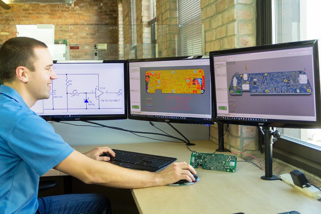
At DMC, we have standardized on Altium Designer as our primary PCB design platform. In addition to our Altium expertise, our team also has hands-on experience with other popular design tools, including KiCAD and Eagle. If your existing project was developed in a different CAD package, we can convert your design to Altium.
How does simulation aid in circuit design?
Simulation helps identify potential issues and optimize designs before physical implementation. It allows for testing component values, circuit performance, and system behavior under various conditions, leading to reduced prototyping costs and time.
What are the main steps in the PCB design process?
The main steps typically include schematic design, component placement, routing (connecting the components with traces), and generating files used for PCB fabrication.
What is the difference between single-sided and double-sided PCBs?
Single-sided PCBs have components on one side of the board, making them simpler and cheaper to manufacture. But on double-sided PCBs, components are placed on both sides, allowing for more complex designs and higher component density.
